Hello friends today I want to continue an old job that I left halfway, because in order to explain it you need to take small steps, to be able to understand it. The world of the physics of the solid and semiconductor states, have an endless number of topics to study, and the deep levels within the forbidden energy gap, is a subject that tends to be very extensive, so as not to overlook details, and that the subject is explained in the best possible way. So today I bring you the second installment of my work I hope you like it.
The speed of electronic capture is proportional to the concentration of electrons n in the conduction band and to the concentration of centers unoccupied by electrons,
, where  depends, in general, on the sections of capture of electrons and holes and is given by:

[Source](https://pixabay.com/es/llev%C3%B3-semiconductor-diodo-luz-rojo-153883/)
<center>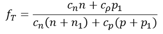</center>
with 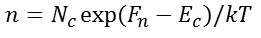 and a similar relation for .  is the Fermi quasi-level for electrons.
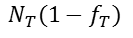
The electronic emission depends  the density of full centers . So the electronic concentration in the driving band varies as:
<center>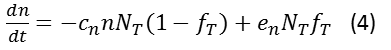</center>
Similar expressions are obtained for voids, so the concentration of voids varies as:
<center>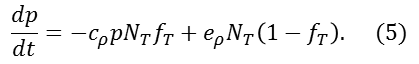</center>
The speed of change of electrons in the traps will be:
<center></center>
where:

The best agreement between the theory and the experiment has been obtained for the speed of optical emission , which is related to the cross-section of photoionization through the expression:
<center>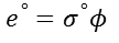</center>
where is the flow of photons used to measure. It is customary to calculate this cross section using the time-dependent perturbation theory.
Deep impurities play a very important role in the semiconductor photoconductivity. When the energy of the incident light is greater than the energy of the forbidden bandwidth, the impurities will contribute by increasing the quantum efficiency of the semiconductor. However, when the energy of the photons is smaller than the energy of the gap, the photoconductivity in the semiconductor will be dominated by the effects of the deep impurities, since these control the recombination rate. In a simple way, photoconductivity by impurities involves a deep impurity that is photoionized by energy light
 that is less than the energy of the forbidden bandwidth of the semiconductor, but greater than the energy of activation of the impurity. If the deep impurity is a donor at a certain energy below the conduction band, the photoinduced carriers are electrons. These electrons remain in the conduction band until they are recaptured by the deep donor, so that the conduction of the semiconductor increases by the applied light. To determine the effect of light on the conductivity, it is necessary to work at low temperatures, that is, in the range of 70 to 180 ° K and apply monochromatic radiation using a mechanical light switch, so that the techniques of Detection with lock-in amplifier to combat noise and drift effects.
## Experimental techniques for the study of deep levels.
Experimental methods for characterizing deep levels in semiconductors can be divided into: steady state methods and transient methods. We will divide the latter into non-spectroscopic methods and spectroscopic methods.
### Stationary state methods.
Stationary-state methods involve measurements under essentially continuous excitation. Among the steady-state methods are: a) admittance spectroscopy method, b) double-source differential photo-capacitance method (DSDP).
_**a) In the admittance spectroscopy method**_, the interest levels are recharged in each half of the cycle of a small c.a. The admittance measurements as a function of the temperature, at two different frequencies, can give a spectroscopy of the deep impurity levels in a Schottky barrier, obtaining information of the energy levels and the capture coefficients of majority carriers. The numerical comparison with capacitance measurements allows to find the concentrations and the types of level (donor or acceptor). Although this is the simplest steady state method, it has the disadvantage of being limited to traps of majority carriers.
_**b) The dual source differential fatocapacitance (DSDP)**_ method allows rapid characterization of deep traps in semiconductors. It consists of continuously illuminating the semiconductor with energy light slightly less than the prohibited bandwidth, which allows the traps to be occupied by both electrons and holes, and then slowly sweep in photon energy with a second source of light disturbing periodically the occupation of the levels by photo ionization, which gives rise to corresponding changes in the capacitance of the union. The DSDP method allows the detection of electronic emission and gap emission processes. The acute characteristics due to individual traps are detected by electronic differentiation with respect to the energy of the photocapacitancy signal; it is for this reason that the technique receives the name of differentiated photocapacitancy of double source. The method is not very sensitive and the data is difficult to interpret.
### Transient methods
In transient methods, information is obtained on the physical properties of the semiconductor, observing the transient response or the relaxation that follows an abrupt disturbance of the system. The techniques developed to date mainly measure capacitance transients in semiconductor or semiconductor semiconductor junctions. The capacitance of the space charge region of a junction changes if the deep traps in the region change their states of charge by the emission or capture of carriers. Very small changes in capacitance (10-3 to 10-4 pF) can be observed by means of capacitance transient techniques. Therefore, information on the behavior of small densities of traps can be obtained in the presence of much higher concentrations of impurities shallow.
We will divide the methods of transients in non-spectroscopic methods and spectroscopic methods, where we talk about spectroscopy in the sense that the signals due to different traps can be distinguished from each other and that they can be reproducible in position when they are plotted against a single variable. Among the main non-spectroscopic methods are: a) thermally stimulated capacitance method (TSCAP). b) photocapacitancy method and e) thermally stimulated current (TSC) method.
# Reference
1.- http://www.sciencedirect.com/science/article/pii/0378436383904321
2.- http://www.tandfonline.com/doi/abs/10.1080/00018738000101396